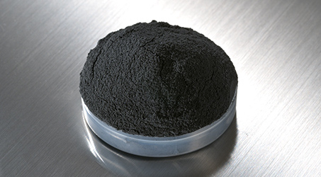
Tungsten and molybdenum products by applications
Tungsten and molybdenum products for semiconductors use
The demand for semiconductors is continuously increasing, driven by IoT, AI, the shift to electric vehicles (EVs), and the ongoing evolution toward a decarbonized society. A.L.M.T. Corp. has established one of the world's largest production systems for molybdenum target materials, which are used as backside wiring barrier materials for LCDs and OLEDs, and is a world leader in the consistent supply of this material.
| Applications |
Sputtering targets, structural components |
|---|
Tungsten and molybdenum products for medical use

Medical equipment is essential for leading healthy lives. A.L.M.T. Corp.'s tungsten and molybdenum also play a crucial role in these devices. Utilizing their high specific gravity, they are used as radiation shielding materials for diagnostic imaging equipment like CT scans and are indispensable in various applications, including catheter reinforcement. Our tungsten and molybdenum products meet the demands for high quality and precision processing due to their importance in human life.
| Applications |
Reinforcing components for catheters, |
|---|
Tungsten and molybdenum products for energy and decarbonization use

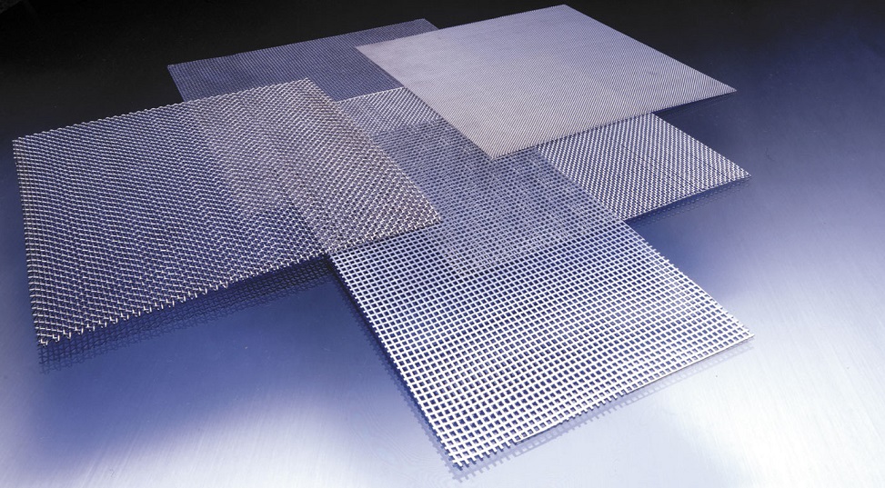
Tungsten and molybdenum are also utilized for power generation from renewable and next-generation energy sources, which are essential for achieving a carbon-neutral society. In addition to mesh products used as wiring formation jigs for photovoltaic power generation, our products are also ideal for divertors in international project of fusion energy (ITER), often referred to as the sun on earth.
ITER also utilizes tungsten, which is resistant to cracking and heat load, based on our core technology.
| Applications |
Fusion reactor divertors, screen meshes for solar cells, etc. |
|---|
Tungsten and molybdenum products for automotive use

Automobiles are essential means of transportation in our daily lives. They are used as filaments for headlamps that brightly illuminate nighttime roads and as balancers for speedometers. Products from A.L.M.T. Corp. are also widely used in jigs and tools required for manufacturing automotive parts, including magnet sintering jigs for motors, electrodes for wire bonding, and raw material powders for various tools.
| Applications |
Filaments for automotive lamps, electrodes for joining wire harnesses, etc. |
|---|
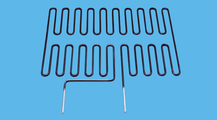
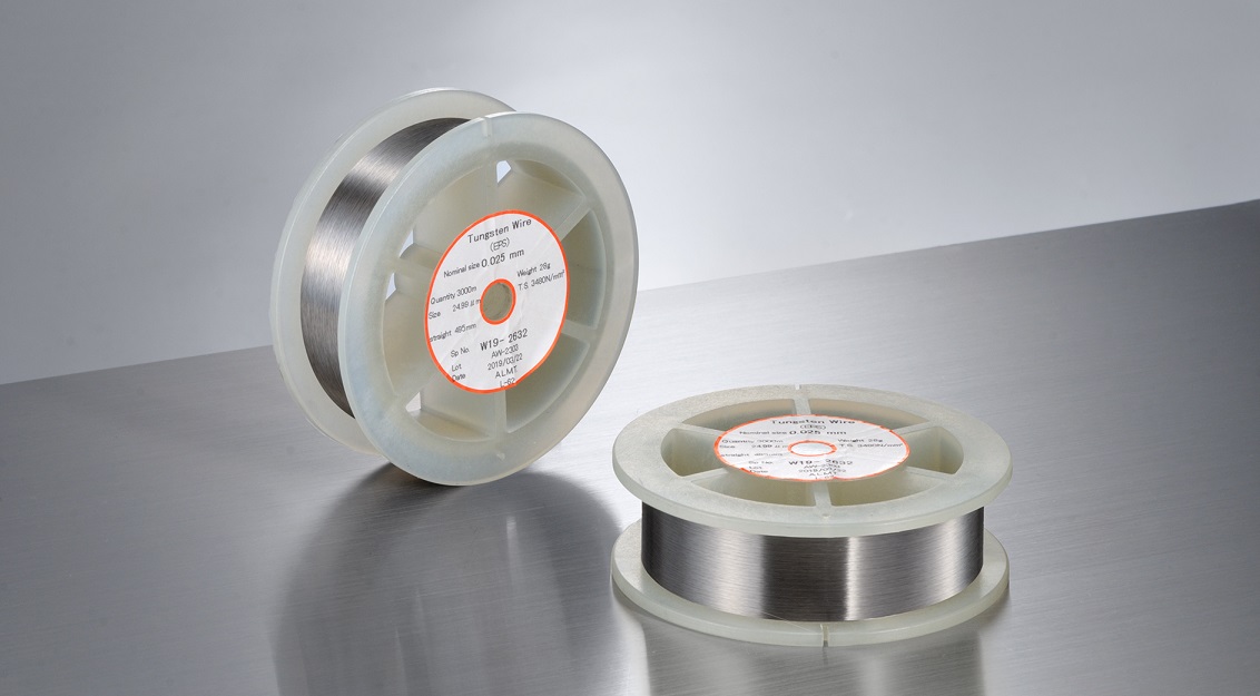
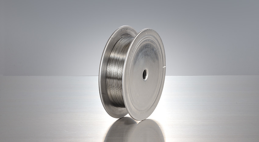
Tungsten and molybdenum products for lamps (lighting) use

Tungsten and molybdenum, both metals with high melting points, are utilized in a wide range of applications from visible light, such as incandescent and high-intensity lamps, to UV light for industrial purposes (exposure) and consumer uses (entertainment) and are deeply integrated into our daily lives. We take pride in our integrated production process, starting from raw materials, and guarantee high quality not only for wires and plates but also for processed products such as electrodes and screw parts.
| Applications |
Electrodes for projector lamps, Filaments for halogen lamps, etc. |
|---|
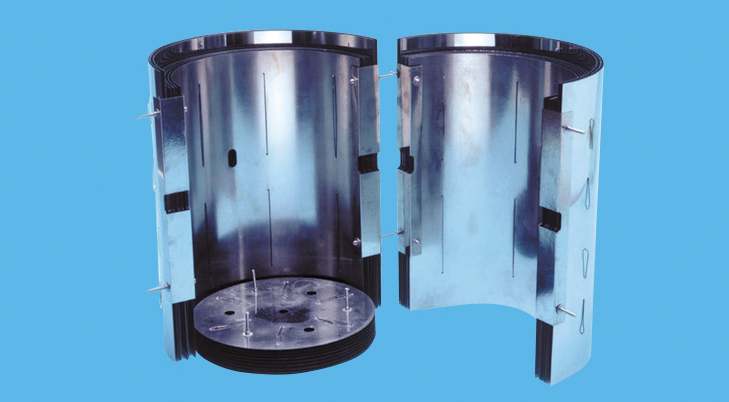
Tungsten and molybdenum products for high-temperature furnaces use
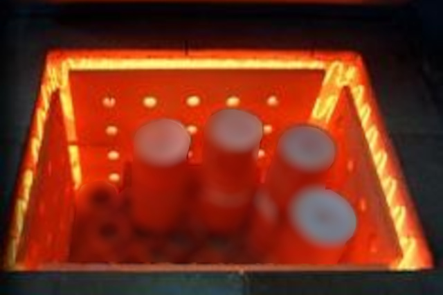
Tungsten and molybdenum, known for their high melting points, are optimal materials for components in high-temperature vacuum furnaces and reduction atmosphere furnaces. Additionally, we offer proprietary materials with excellent resistance to deformation, even at elevated temperatures, contributing to a longer service life. We can also design and propose products tailored to meet your specific requirements.
| Applications |
Components for high-temperature furnaces (Heaters, Reflectors), etc. |
|---|
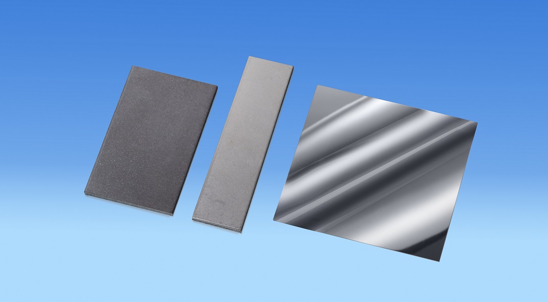
Tungsten and molybdenum products for glass use
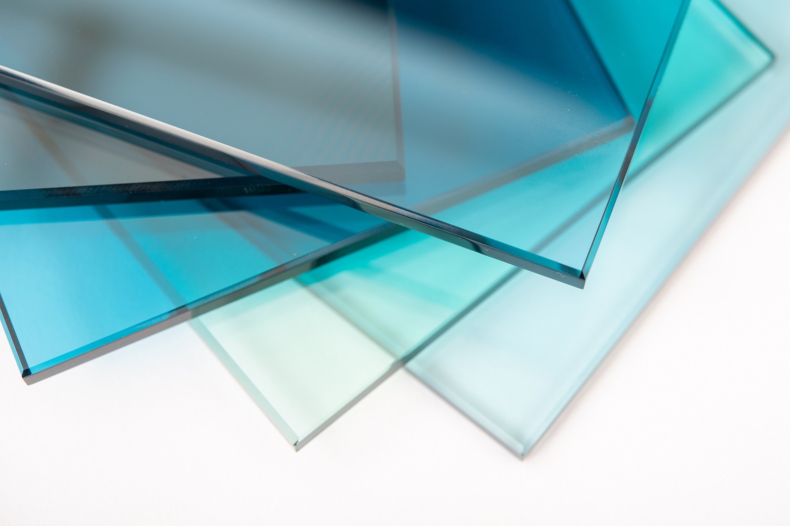
A.L.M.T. Corp.'s tungsten and molybdenum products are also utilized in the manufacture of commonly seen glass products, such as windows and water tanks. Leveraging their high melting points and ability to perform at elevated temperatures, they are employed as furnace components and jigs for melting furnaces that reach temperatures of 1,200 to 1,400℃.
| Aoolications |
Structural jigs for glass melting furnaces, etc. |
|---|
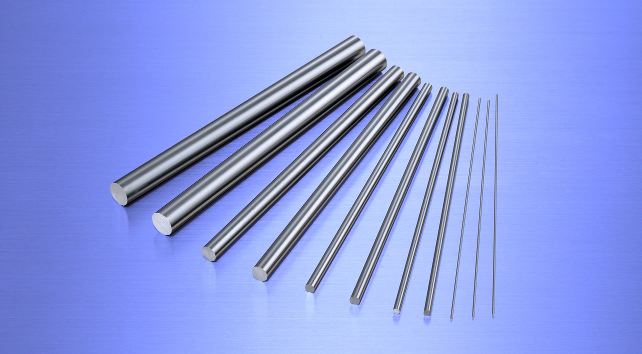
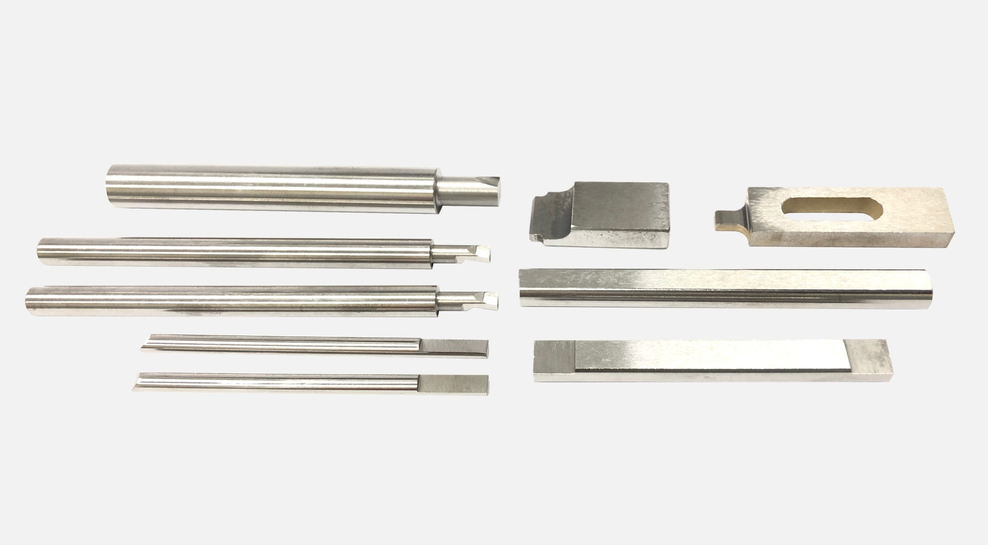
Tungsten and molybdenum products for welding, cutting and tools use
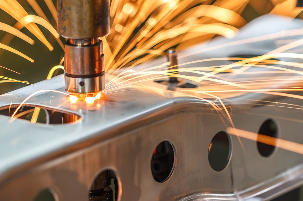
When welding metals, TIG welding is employed for applications requiring a beautiful finish and precise results, with our tungsten serving as the electrode. Additionally, tungsten and molybdenum products with high melting points are well-suited for pressure welding electrodes used in automotive wiring and electric discharge machining wires.
| Applications |
Electrodes for welding and pressure welding, Cut wire, etc. |
|---|
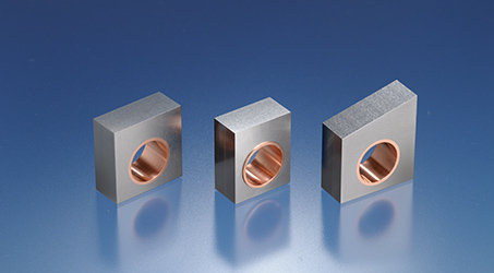
Cu-W(銅-タングステン)放熱基板ラインアップ
スクロールで表全体をご覧いただけます。
| 材質 | 名称 | 組成 | 特徴 | 平均線膨張係数 R.T.~800℃[ppm/K] |
熱伝導率 R.T.[W/(m・K)] |
|---|---|---|---|---|---|
| Cu-W | W-6 | 94W-6Cu | 熱膨張率を低く抑えたCu-Wであり、GaAsやGaNに熱膨張率が近く、熱膨張のミスマッチを制御します。 | 6.4 | 141 |
| W-10 | 89W-11Cu | アルミナと熱膨張率の整合をとっており、アルミナを用いたセラミックスパッケージに広く用いられています。 | 7.9 | 174 | |
| W-15 | 85W-15Cu | ベリリアセラミックと熱膨張率の整合をとっており、ベリリアを用いたセラミックスパッケージに広く用いられています。また、熱膨張率がアルミナとコバールの中間値のためアルミナとコバールの両方用いたパッケージにも広く用いられています。 | 8.6 | 184 | |
| W-20 | 80W-20Cu | コバールと熱膨張率の整合をとっており、コバールを用いたメタルパッケージに広く用いられています。 | 9.8 | 200 | |
| W-10N | 89W-11Cu | アルミナと熱膨張率の整合をとっており、アルミナを用いたセラミックパッケージに広く用いられています。W-10Nは専用金型の作製により、外周加工レスCu-W(ニアネットCu-W)を提供できます。 | 7.9 | 200 | |
| W-10T | 89W-11Cu | 熱膨張率はW-10と同じですが、特別な製法により熱伝導率を向上させています。また、反りを小さく抑えることが可能なため高出力レーザー用のサブマウント用途に広く使用されています。 | 7.9 | 205 |
Cu-Mo(銅-モリブデン)放熱基板ラインアップ
スクロールで表全体をご覧いただけます。
| 材質 | 名称 | 組成 | 特徴 | 平均線膨張係数 R.T.~800℃[ppm/K] |
熱伝導率 R.T.[W/(m・K)] |
|---|---|---|---|---|---|
| Cu-Mo | CM-15 | 85Mo-15Cu | 熱膨張率を低く抑えたCu-Moであり、GaAsやGaNに熱膨張率が近く、熱膨張のミスマッチを制御します。 | 7.6 | 148 |
| PCM30 | 70Mo-30Cu | 熱膨張を低く抑えたCu-Moですが、圧延やプレス加工などコストに優れた製法が適用可能です。 | 7.5 | 195 | |
| PCM35 | 65Mo-35Cu | アルミナと熱膨張率の整合をとっており、アルミナを用いたセラミックパッケージに広く用いられています。 | 7.8 | 210 | |
| PCM40 | 60Mo-40Cu | 熱膨張率がデバイス(Si、GaAs、GaN、SiC)と銅やアルミの中間値のため、銅板やアルミ板上にデバイスを実装する場合の応力緩衝材として広く用いられています。 | 8.2 | 220 | |
| RCM60 | 40Mo-60Cu | 熱膨張率がデバイス(Si、GaAs、GaN、SiC)と銅やアルミの中間値のため、銅板やアルミ板上にデバイスを実装する場合の応力緩衝材として広く用いられています。 | 10.5 | 275 |
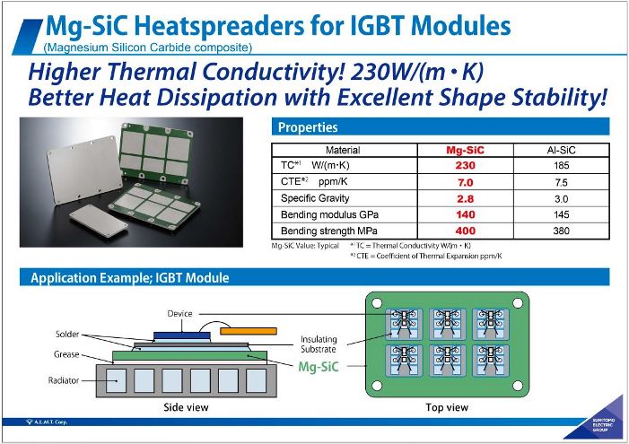
Mg-SiC(マグネシウム合金-炭化珪素)放熱基板ラインアップ
スクロールで表全体をご覧いただけます。
| 材質 | 名称 | 組成 | 特徴 | 平均線膨張係数 R.T.~120℃[ppm/K] |
熱伝導率 R.T.[W/(m・K)] |
|---|---|---|---|---|---|
| Mg-SiC | Mg-SiC | 18Mg-SiC | 軽量のため大型基板での使用に適しています。 さらに反りが安定しており、高熱伝導とあわせ放熱性に優れています。 |
7.0 | 230 |
Mo(モリブデン)放熱基板ラインアップ
スクロールで表全体をご覧いただけます。
| 材質 | 名称 | 組成 | 特徴 | 平均線膨張係数 R.T.~800℃[ppm/K] |
熱伝導率 R.T.[W/(m・K)] |
|---|---|---|---|---|---|
| Mo | Mo | Mo | 半導体(Si、GaN、SiC)に熱膨張が近く、半導体への熱ストレスを低減するために広く用いられます。 | 5.7 | 142 |
Cu-Diamond( 銅-ダイヤモンド)放熱基板ラインアップ
スクロールで表全体をご覧いただけます。
| 材質 | 名称 | 特徴 | 平均線膨張係数 R.T.~400℃[ppm/K] |
熱伝導率 R.T.[W/(m・K)] |
|---|---|---|---|---|
| Cu-Diamond | DC60 | 熱膨張率を化合物半導体(GaAs,GaN)に合わせた高熱伝導ヒートシンクです。 | 6.0 | 550 |
| DC70 | 6.5 | 500 |
AlN(窒化アルミニウム)放熱基板ラインアップ
スクロールで表全体をご覧いただけます。
| 材質 | 名称・組成 | 特徴 | 平均線膨張係数 R.T.~400℃[ppm/K] |
熱伝導率 R.T.[W/(m・K)] |
|---|---|---|---|---|
| AlN | AlN(200W) | 絶縁やパターン回路が必要な場合に有用です | 4.5 | >200 |
| AlN(170W) | 4.5 | >170 |
CPC(銅-銅モリブデン-銅)放熱基板ラインアップ
スクロールで表全体をご覧いただけます。
| 材質 | 名称 | 組成 | 特徴 | 平均線膨張係数 R.T.~800℃[ppm/K] |
熱伝導率 R.T.[W/(m・K)] |
|---|---|---|---|---|---|
| CPC | CPC141 | Cu/Cu-Mo/Cu | アルミナと熱膨張率の整合をとっており、アルミナを用いたセラミックパッケージに広く用いられています。 | 7.6 | 200 |
| CPC232 | Cu:Cu-Mo:Cu=2:3:2(厚み)で積層し、熱膨張率と熱伝導率を調整した材料です。 | 8.4 | 235 | ||
| CPC111 | Cu:Cu-Mo:Cu=1:1:1(厚み)で積層し、熱膨張率と熱伝導率を調整した材料です。 | 9.8 | 260 | ||
| CPC212 | Cu:Cu-Mo:Cu=2:1:2(厚み)で積層し、熱伝導率を300W/(m・K)に高めた材料です。高出力デバイス(GaN、SiC)の性能発揮のため広く用いられています。 | 12.1 | 300 | ||
| CPC-300 | 熱伝導率が300W/(m・K)と非常に高く、高出力デバイス(GaN、SiC)の性能発揮のため広く用いられています。0.5mmの薄板対応も可能です。 | 12.1 | 300 |
CVDダイヤモンド(単結晶ダイヤモンド)放熱基板ラインアップ
Al-SiC(アルミ-炭化珪素)放熱基板ラインアップ
スクロールで表全体をご覧いただけます。
| 材質 | 名称 | 組成 | 特徴 | 平均線膨張係数 R.T.~400℃[ppm/K] |
熱伝導率 R.T.[W/(m・K)] |
|---|---|---|---|---|---|
| Al-SiC | β8 | 70SiC-30Al | 専用金型により加工を必要とせず、安価に製造できます。 パッケージの種類により熱膨張率が可変です。 |
8.0 | 140 |
| β9 | 65SiC-35Al | 9.0 | 130 | ||
| β14 | 45SiC-55Al | 14.0 | 160 |
Ag-Diamond(銀-ダイヤモンド)放熱基板ラインアップ
スクロールで表全体をご覧いただけます。
| 材質 | 名称 | 特徴 | 平均線膨張係数 R.T.~800℃[ppm/K] |
熱伝導率 R.T.[W/(m・K)] |
|---|---|---|---|---|
| Ag-Diamond | AD90 | Cu-Diamondよりも高い熱伝導率(600W/(m・K))を有しており、50×50mm2の大面積の用途へも適用可能です。 | 10.5 | 600 |
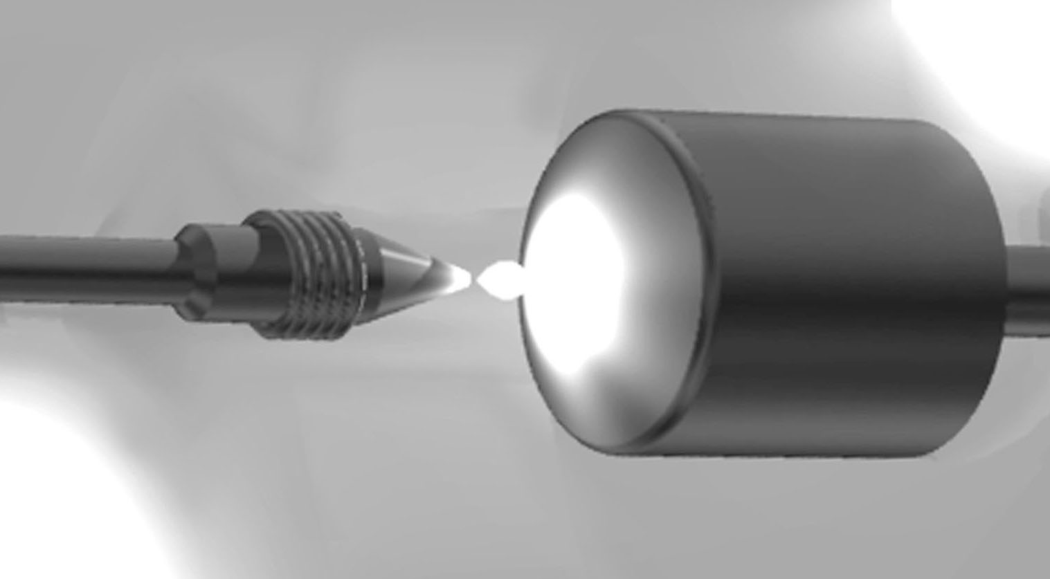
バーレーザ実装イメージ
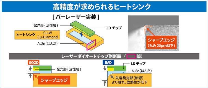
ヒートシンクとなる AIN、Cu-W、Cu-Diamond はシャープエッジ(ピン角)に加工できるため光路を妨げず、エッジ先端部で発光する LD 部の放熱性を高めます。また、はんだ流れを制御する技術により、安定したレーザ性能を実現します。
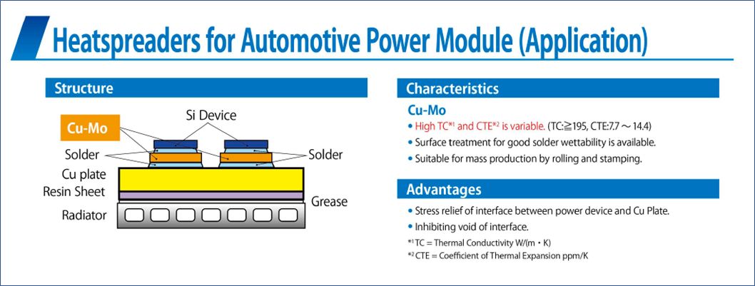
自動車用パワーモジュール(Cu-Mo)
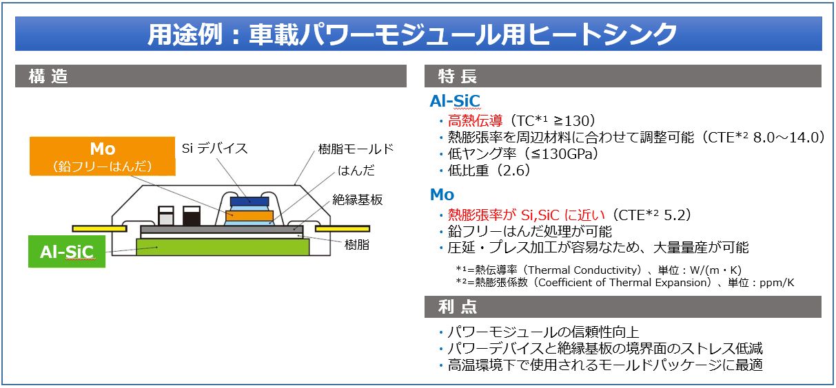
自動車用パワーモジュール(Mo)
IGBTモジュール
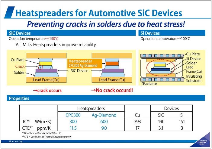
自動車用SiCデバイス
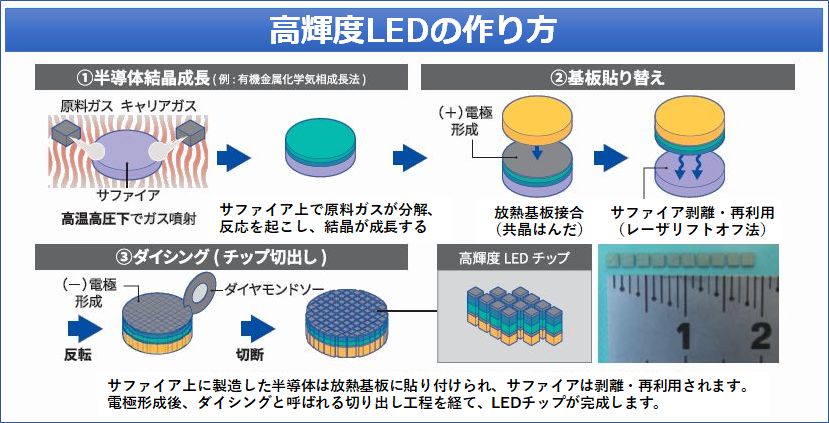
高輝度LEDの作り方
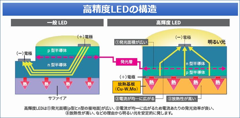
高輝度LEDの構造
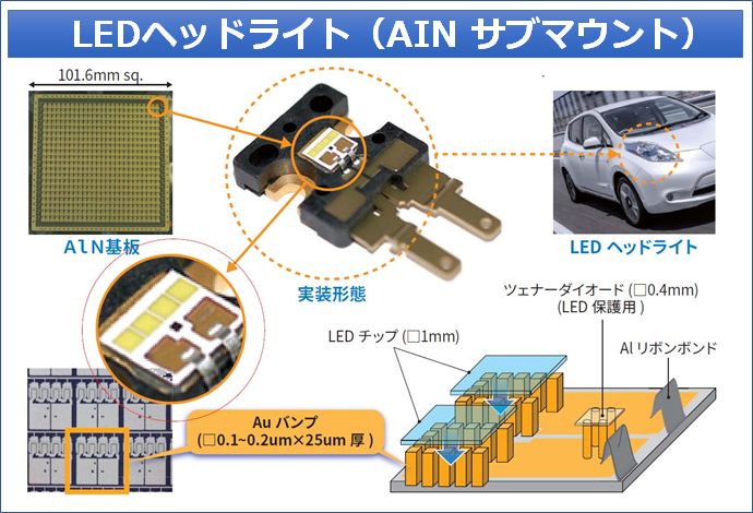
LEDヘッドライト(AIN サブマウント)
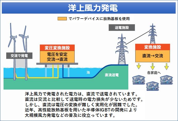
洋上風力発電